Samsung SDI Improves PCB Development

Samsung SDI Improves PCB Development

Samsung SDI Saves Six Million USD Annually with Altair PollEx™

About the Customer

Samsung SDI is headquartered in South Korea, as a global market leader in the high technology and environmental battery industry. Samsung SDI has a 40-year history, spanning from vacuum tubes, to large plasma display panels (PDPs), to high-tech cathode ray tubes (CRTs) and digital displays.

Today, Samsung SDI is a top player as an energy and materials provider of rechargeable batteries for the IT, automotive, energy storage systems (ESS), and electronic material industries.

Their Challenge

When Samsung SDI transitioned to the electronic materials business, several challenges surfaced that needed to be addressed. The company had to move from digital display control circuits to battery control circuits, requiring a different approach to new electronic designs and related printed circuit board (PCB) manufacturing technologies.

A strong solution for PCB design review, and verification was needed for existing and new products. Also, after acquiring a key player in the automotive battery pack business, Samsung SDI needed a solution that could setup and deploy PCB design review and verification where the design rules and user environment were centrally managed.


“PollEx PCB Verification solution was initially adopted to reduce manufacturing defects and human errors of engineers, and thanks to it we could significantly reduce development and manufacturing costs.”

– JungWon Lee, Chief Researcher, Samsung SDI

Our Solution

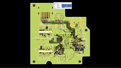
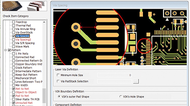
Samsung SDI evaluated Altair PollEx for PCB design review (PCB Modeler) and verification (PCB Verification). Paying special attention to the supported design rules for manufacturing (DFM) and design for electrical engineering (DFE), the objective was to manage and enhance the process from design to manufacturing.

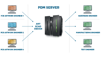
With the user-friendly collaboration capabilities, PollEx allowed teams of PCB designers, hardware engineers, test engineers and manufacturing engineers to communicate overseas. Samsung SDI needed a solution that could also be used by all branch locations, but allow the design rules and verification environment to be centrally managed.

Altair worked closely with Samsung SDI engineers to ensure the PCB verification solution could be used for existing and new products with different verification requirements. Thanks to PollEx, after two months Samsung SDI had an efficient collaboration environment with PCB verification capabilities that could be used by multiple teams. With this enronment in place, PCB artwork engineers can upload PCB layout designs to a PDM server, including the designs in PollEx’s format. All engineers can then review the PCB designs with PCB Modeler while running PollEx PCB Verification tools.

Results

With PollEx, Samsung SDI successfully collaborates from a central solution with PCB design review and verification capabilities. This saves an estimated six million USD a year thanks to a reduction of design iterations from 20 to nine and number of revision checks from six to three.

Samsung SDI uses PollEx for PCB design review and uses DFM to detect manufacturing faults in the early design stage. They expanded the use of PollEx with DFE, to detect electrical failures earlier in the design process. In the future, analysts will use PollEx Solvers for signal and power integrity, and for thermal analysis.