Altair® PollEx™ Applications
Global industry leaders rely on PollEx’s printed circuit board (PCB) simulation solution to streamline operations, boost productivity, and foster collaboration for their PCB design review processes. PollEx’s integrated workflows ensure companies meet their performance, reliability, and compliance targets while minimizing redesign, prototyping, and time to market.
Learn More About PollExCollaborate, Validate, and Simulate with PollEx
Learn More
Collaborative PCB Design Review
PollEx simplifies PCB design reviews across multiple electronic design automation (EDA) tools and mechanical aspects. With version control and collaborative features for comparing schematics and PCB data, reviewers can rapidly detect faults and resolve issues early in the PCB design layout process without needing expensive electronic computer-aided design (ECAD) licenses.
ECAD Integration, Simplified
PollEx offers a unified viewing, collaboration, and verification environment. Import from all major ECAD vendors and ensure design data and rules are normalized for consistency. Search and select design objects such as components, pins, and nets based on all technical attributes.
Schematic and PCB data
Access all schematic attributes on symbols and nets to identify disconnects or mismatches between schematic and PCB design data or bill-of-materials (BOM) with cross-highlighting and cross-selection capabilities.
Design Review and Annotation
Collaborate on design reviews across all departments and contributors within the same normalized design set – regardless of EDA source data. Share redlined issues with comments while keeping critical intellectual property in-house and protecting it with design subsets for external project contributors.
Discover how PollEx empowers companies like Samsung.
Learn More
Design Inspection and PCB Verification
PollEx surpasses standard ECAD capabilities to accelerate PCB design optimization. Multidisciplinary teams can collaborate at the logical schematic capture, design, and BOM levels and leverage smart documentation for fast, error-free PCB verification that delivers high-quality designs to market faster.
Design for Manufacturing (DFM)
PollEx supports more than 500 DFM rules and related integrated checks, far exceeding standard ECAD checks, including PCB technical cleanliness checks for particle impurity classification, component category checks for part placement, and PCB route pattern checks. These and other DFM checks ensure designers deliver safe, high-quality PCBs with fewer prototypes. Learn more about PCB technical cleanliness challenges.
Design for Assembly (DFA)
PollEx DFA verifications provide a collaborative workflow between design teams and assembly machine manufacturers. With over 50 dynamic and situation-driven checks, design teams can optimize and accelerate assembly processes while avoiding issues such as collisions, lead problems, placement errors, and component-board mismatches. Additionally, teams can export any needed fabrication, mounting, paneling, and test data directly to the production line machinery, ensuring a smooth PCB production process.
Design for Electric (DFE) Performance
PollEx's rule-based PCB verification solution tool, tailored for electrical engineers and designers, supports over 280 electrical, EMC and high-speed design rule checks required by advanced technologies, ideal for diverse sectors like transportation, aerospace, consumer electronics, and medical devices.
Experience the Power of PollEx
Try Now
PCB Thermal Analysis
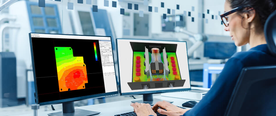
PollEx provides fast board-level thermal analysis workflows for any skill level. With a streamlined setup, efficient computations, and precise results, teams can quickly identify thermal hotspots and optimize thermal performance, including the system-level PCB placement.

System Analysis and Optimization for Electronic Circuit Boards
PollEx is integrated with other Altair and third-party physics simulation tools. Seamlessly transfer PollEx PCB board simulation results to the Altair® SimLab® multiphysics design environment for additional evaluation. Perform detailed 3D thermal analysis considering all elements of a PCB, including 3D components, PCB materials, and copper structures on all layers. Simulate systems with multiple PCBs within enclosures with various fan or heat sink cooling options. SimLab’s process-oriented workflows empower users of all levels to simulate structural stress, vibration, and drop test performance for fast, accurate results. And with Altair® Feko®, perform detailed EMI/EMC analysis.
How can we help you accelerate your electronic systems development?
Contact UsFeatured Resources

Guide to Electronic System Development
Manufacturers today are tasked with designing smart, connected products at a breakneck pace to stay ahead of the competition. As performance demands continually increase, packaging sizes become smaller, and device connectivity becomes more critical, schematic engineers and product designers need ways to make efficient design decisions and collaborate with one another to optimize complex interconnected mechanical and electromagnetic systems. To develop the next generation of smart products, organizations are turning simulation to improve device performance and drive profitability.

Meeting PCB Technical Cleanliness Challenges with Altair® PollEx™
PCB technical cleanliness design verification is crucial for maintaining product reliability and lifespan. It is especially vital in the automotive and aerospace industries, where contaminants in critical components can lead to severe malfunctions, costly recalls, and non-compliance with stringent industry standards.
Altair Pollex addresses the challenges of technical cleanliness in PCB designs. By implementing verification processes early in the design stage, companies can identify, classify, address potential issues within PCB designs, fostering a more efficient development pathway.

Tackling EMI/EMC Challenges: One Rule at a Time
If you’re not a signal integrity (SI) expert, the thought of EMI/EMC issues might bring you chills. As PCB simulation tools continue to improve, it’s important to incorporate signal integrity checks early in the design process. Instead of waiting for the analysis results after laying out your PCB, why not implement best practices into your verification process.In this workshop, we will look at common EMI/EMC issues, and how they can be traced back to design best practices. We also look at how we can use rule based verification to automatically check for indicators, saving time and money. This workshop is meant for beginner to mid-level PCB designers and Signal Integrity engineers. The purpose of this workshop is to add a skillset that helps free up the time of the Signal Integrity Expert. This workshop also encourages users to add best practices into their current workflow by adopting this methodology. This workshop can be done with generic DFE and DFM tools. Attendees will learn:
- The effect of PCB miniaturization on signal integrity.
- Common DRC setups to identify EMC errors early.
- How to improve quality by incorporating automated verification for EMI/EMC
Presented by Harry Kennedy, Technical Specialist Electronic System Design| Altair, at the ATCx Electronics for Engineers in October 2023, 17 mins

PCB Verification for Reliable and Safe Electronics
PCB verification identifies and suggests corrections early in the design stage. Through verification, users check a pre-prototype layout design against geometrical design requirements and best practices. As an outcome, the risk for product functional, electrical, and assembly issues is reduced. PCB verification is addressing harsh operating conditions for a vehicle, such as temperature fluctuations, humidity, vibration, and electromagnetic interference through electrical validity and manufacturability.
Presented by Niranjan Anant Bhat, Product Engineer| Altair, and Marek Jableka, Senior Technical Specialist Electronic System design I Altair, at the ATCx Electronics for Engineers in October 2023, 23.3 mins

